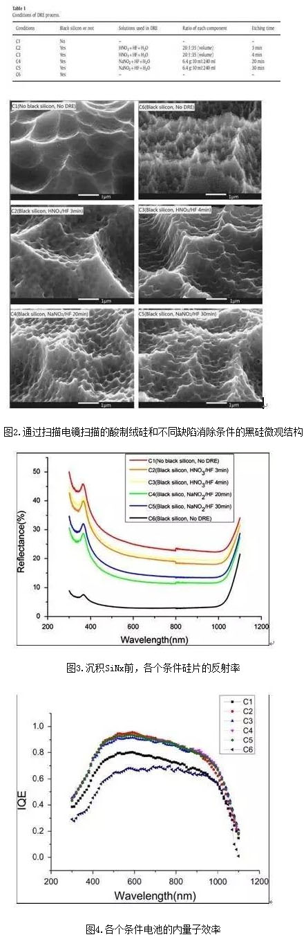
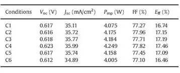
In order to increase the absorption of incident light by solar cells, polysilicon black silicon has been successfully produced using plasma immersion ion implantation using SF6 and O2. This experimental study compares the differences in eliminating black silicon defects under several different conditions. Eliminating black silicon surface defects can reduce surface area and etch damage and reduce surface recombination. The surface structure, reflectance and internal quantum efficiency of black silicon were studied by field emission scanning electron microscope, spectrophotometer and quantum effect tester, respectively. The results show that the number and height of hill peaks on black silicon surface decrease with the increase of etching time; the reflectance of black silicon surface decreases with the increase of the number and height of hill peaks. The internal quantum efficiency (IQE) and electrical performance of the batteries after eliminating the defects are greatly improved compared to the batteries without the elimination of defects. The highest efficiency black silicon cell efficiency, open circuit voltage, and short circuit current density were 17.46%, 623mV, and 35.99mA/cm2, respectively, which was 0.72% higher than that of the traditional acid-studded polysilicon solar cell. 1 Introduction Reducing the surface reflectivity of silicon wafers to increase light absorption is an important direction for polysilicon solar cells to improve conversion efficiency. Deposition of anti-reflection layers (such as SiNx) is a method that can effectively reduce reflections, but surface texturing is a more stable and effective anti-reflection method. In industrial production and experimental research, monocrystalline silicon is anisotropically etched in lye, and the pyramidal structure on the surface of the silicon wafer can effectively reduce the light reflectance on the surface of the silicon wafer. However, the polysilicon crystals are irregular and areotropic, and they cannot be napped in lye, but are napped in an acid solution. The reflectivity of the monocrystalline silicon after texturing is about 11%, but the reflectivity after polysilicic acid texturing is about 25%, and the reflected light loss is still large. In order to further reduce the reflectivity of the surface of silicon wafers, especially polysilicon wafers, many attempts have been made to fabricate nanostructures on the surface of silicon wafers. The silicon wafers appear to be black, which is known as black silicon. Kontermann et al. used a femtosecond laser pulse process to produce single crystal black silicon solar cells. Dimitrov and Du chemically produced random nanoscale pyramids in a mixture of acidic Na2S2O8 and AgNO3, with a conversion efficiency of 17.5%. Black silicon can also be fabricated using reactive ion etching and plasma immersion ion implantation methods. Kumaravelu et al. found that ion etching can cause defects in nanostructures and that nanostructures increase the surface area of ​​the silicon wafer, which can reduce the minority carrier lifetime on the wafer surface. Therefore, it is necessary to eliminate defects on the surface of the black silicon to optimize the electrical properties of the battery. Lee et al. produced a black silicon solar cell using a reactive ion etching method. After the defect was eliminated, the cell efficiency was as high as 16.32%, which was 0.7% higher than that of the conventional acid cellulosic cell. Visible defect elimination process can greatly enhance the electrical properties of black silicon solar cells. In this paper, in order to study the effect of defect elimination process on the electrical properties of black silicon solar cells, we used plasma immersion ion implantation to fabricate black silicon solar cells and did several experimental comparisons of defect removal process conditions. 2 experimental design The polysilicon chip used in this test is 156mm*156mm, P-type doped, and its thickness is 200±20μm. Figure 1 shows the production process of polycrystalline black silicon solar cells. First, the surface damage of the silicon wafer was removed in a 10% NaOH solution at 80°C. Subsequent use of plasma immersion ion implantation method of texturing. The flow rate of SF6/O2 into the vacuum reaction chamber was 3:1 during texturing, and the radio frequency and power used were 13.56 MHz and 900 W, respectively. There was no DC bias and the etching time was 4 minutes. The black silicon defects were then eliminated using different process conditions (Table 1) at 23°C. All solar cells use POCl3 diffusion at 825°C. The edge of the wafer was then etched using CF4 and O2 plasma for 40 minutes. Phosphorous silica glass was removed in a volume fraction of 10% HF solution. SiNx was deposited to a thickness of 80 nm using plasma-enhanced chemical vapor deposition (PECVD). Finally, the screen printing and sintering are made into a battery. Scanning electron microscopy (SEM) was used to study the micro-morphology of black silicon. The reflectivity of black silicon surface was measured by a UV-VIS-NIR spectrophotometer with an integrating sphere detector. The SolarCellScan 100 quantum effect test system was used. Test the IQE of solar cells. 3 experimental results and discussion Figure 2 is a black silicon surface topography with six different conditions. The density and height of the nano-hills on the surface of the C2 to C6 wafer are different. C1 is an acid velvet and has no nanoscale structure on the surface. C6 is the original black silicon without defect removal treatment. The density and height of the surface hill peaks are relatively large. Nanostructures are formed by etching ions and masks. It can be seen that the density and height of the C5 to C2 hill peaks continue to decrease. The chemical reaction to eliminate defects is completed in two steps. First, the surface of the silicon wafer is oxidized by HNO3 or NaNO2 to produce an oxide layer on the surface of the wafer. The oxide layer is then etched away by HF, resulting in a reduction in the density and height of the hill. C2 and C3 conditions on the surface of the black silicon hill peak concentration and height lower than the C4, C5. This is because HNO3 has stronger oxidizing power than NaNO2. Regardless of the type of etching solution, the longer the reaction time, the lower the density and height of the small peak. UV-VIS-NIR spectrophotometer with an integrating sphere detector was used to test the reflectivity of the black silicon surface in the wavelength range of 300-1100 nm, as shown in Fig. 3. The average reflectance is calculated by the following formula R(λ) is the total reflectance, and N(λ) is the sunlight flux under the AM1.5 standard. It can be found that the black silicon without the defect removal process has the lowest reflectivity and the average reflectance is 3.99%. The reflectivity of C2 to C5 increased in turn, but they were all lower than the reflectivity of 25.31% of acid-reduced silica. Regardless of the etching solution, the density and height of the small peak will gradually decrease with the extension of the chemical reaction time. The average reflectance of C2 was 20.99%, C3 was 22.07%, and the reflectivity of C3 was higher than that of C2; the reflectance of C4 was 13.39%, the C5 was 15.62%, and C5 was higher than C4. This phenomenon can be attributed to the following two aspects: First, the small hill on the black silicon surface can increase the light reflection time, and the chance of the silicon piece absorbing light is greater; secondly, due to the close proximity of the diameter of the small peak and the wavelength of visible light, zero-order diffraction The stripes are very weak. It can be seen that the reflectance of condition C6 to C1 gradually increases. This phenomenon can be attributed to the fact that as the density and height of the hill peak are reduced, the reflection time of the incident light will be shortened and the interference effect will be weakened. Figure 4 shows the internal quantum efficiencies of C1 to C6 for incident light wavelengths in the range of 300-1100 nm. It can be seen that the internal quantum efficiency after the elimination of defects is much higher than that of untreated ones. The main reasons for this phenomenon are the following two aspects. First of all, the black silicon that does not eliminate defects has a high density and height of surface hill peaks, increasing the surface area. The black silicon surface has many effective composite centers such as dangling bonds, trapping centers, etc. The larger the surface area, the more complex centers there are. Secondly, the plasma etching of the black silicon surface will produce defects on the black silicon surface. These defects are also effective recombination centers. These defects can be etched away after being treated with a defect elimination process to improve the collection of the minority sons. The defect-free black silicon has a lower internal quantum efficiency than the acid-based fuzz. This shows that the black silicon surface compound without eliminating defects is higher than the acid velvet. At the same time, it can be found that there is no significant difference in the quantum efficiency of black silicon (C2-C5) after eliminating defects. The black silicon etched by HNO3/HF has a high reflectivity, a small surface area, so the surface damage is small, and the black silicon etched by NaNO2/HF has a low reflectivity, and the surface area is large, so the surface damage is large. The two factors of black silicon reflectivity and surface damage etched by the two solutions reach equilibrium, so there is little difference in internal quantum efficiency. Table 2 is the electrical performance data for each experimental condition. As can be seen from the table, the conversion efficiency of condition C4 is the highest. The conversion efficiency, open circuit voltage, and short circuit current density were 17.46%, 623 mV, and 35.99 mA/cm2, respectively. This conditional reflectance is not the lowest. From this data, we can see that for higher conversion efficiency, we need to find the equilibrium point of the surface reflectance and the surface compounding. Due to the large surface area and defects created by plasma etching, very low reflectivity will inevitably lead to very high surface recombination. For example, the efficiency of condition C6 is 0.28% lower than that of an acid flock battery. The condition conversion efficiency after all the defects were eliminated was higher than that of the acid cellulosic batteries, and the results of other people's studies were also the same. For example, Shim et al. found that black silicon cells fabricated by reactive ion etching are also less efficient than acid cellulosic batteries. However, the efficiency of this black silicon after the elimination of defects has greatly improved. The efficiency of condition C4 is the highest, which is 0.72 higher than that of an acid flock battery. Table 2 Electrical performance data for conditions C1-C6. Voc open circuit voltage, Jsc short circuit current density, Pmp maximum power, FF fill factor, Eff photoelectric conversion efficiency. 4 Summary Polycrystalline black silicon was successfully fabricated using plasma immersion ion implantation and several different defect removal process conditions were investigated. The density and height of the small peaks decrease as the processing time increases. The surface reflectivity of the silicon wafer decreases as the density and height of the hill peak increase. All experimental conditions of silicon wafers were made into solar cells. The quantum efficiency of the battery after the elimination of the defect is improved, which is attributed to the reduction of the surface recombination. In addition, the battery conversion efficiency after the elimination of the defects was higher than that of the batteries without the elimination of the defects and the acid piled batteries. The conversion efficiency of condition C2 (NANO2/HF/H2O, 20 minutes) was the highest, and the conversion efficiency, open circuit voltage, and short circuit current density were 17.46%, 623 mV, and 35.99 mA/cm2, respectively. (Zhao Pengsong, Li Ji, Ma Zengzhi, Wang Shangxin, Liu Xiao, Wang Tian, ​​Wang Yuxiao)
Acid dye refers to an acid group in the dye molecule, also known as an anionic dye, which can be combined with an amino group in a protein fiber molecule by an ionic bond, and is suitable for acidic, weak acid or neutral conditions. Mainly azo and anthracene structures, a few are aromatic methane structures. Dyes and colors are generally compounds which are self-colored and which provide a clear and strong color to other substances in a molecular state or in a dispersed state.
Acid Dyes Jinan Huijinchuan Chemical Industry Co., Ltd. , https://www.hjcchemical.com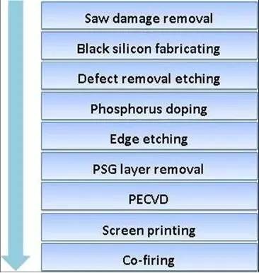
Figure 1. Production process for polycrystalline black silicon solar cells